Photonic-plug technologies have the ability to enable high-speed optical connectivity for next-generation data centers, high-performance computing, 5G, sensor, and other datacom applications.
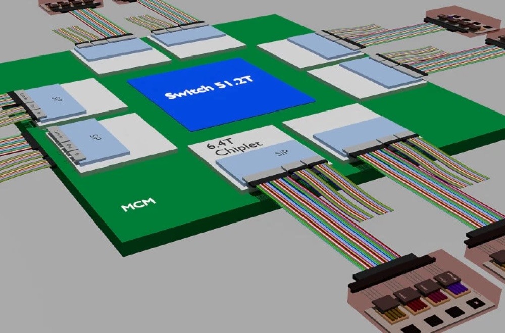
A small Israeli start-up focusing on fiber-to-silicon connectivity solutions for ultra–high bandwidth applications has raised $8 million that will allow it to proceed to production and commercialization of its technology. Teramount (Jerusalem, Israel) recently demonstrated a 100x improvement in tolerance for assembling fiber to silicon chips compared with existing technologies. “This investment is a major vote of confidence in our breakthrough photonic-plug technology, which will open the door to next–generation tech set to fulfill the promise of silicon photonics in date centers, mobility 5G and beyond,” said Hesham Taha, CEO of the company. “Our recent results in the development of co-packaged switches are a crucial first step and now with this funding , we are readying to take the giant leap forward to productization and market impact.” Teramount’s project is targeting one of the most significant challenges of next generation data center co-packaged switches: the need to connect in a completely reliable and cost effective way hundreds of fibers to a single switch chip at high yield. And Taha suggests the technology will also allow breakthroughs in 5G sensors and chip-to-chip optical connectivity.

A co-packaged switch with hundreds of fiber connections.
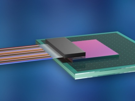
The A-round funding was led by Grove Ventures and also included Amelia Investments, as well as the former executive VP of Intel and company chairman David Perlmutter. Teramount was founded in 2013, but started serious development early 2015. Taha’s cofounder is the company’s CTO Abraham Israel. The company’s approach has developed a way to simplify the packaging of silicon photonics chips. Instead of using active alignment — where an external laser is required to carefully align fiber to the optical die — a form of passive alignment is being deployed. The solution involves two main elements: a PhotonicsPlug that is flip-chipped on to the silicon photonics die while still part of a wafer; and a “bump,” a design element added on to the silicon photonics chip next to the optical waveguide. The main PhotonicsPlug component is a silicon die comprising optics that manipulates the beam using self-aligning optics and focuses it on to the silicon photonics chip via a glass spacer. The die also has V-grooves to interface the single-mode ribbon fiber. The resulting tolerance with which the die can be attached to the silicon photonics wafer is said to be plus or minus 20 microns in each of the three dimensions so that standard flip-chip machines can attach the PhotonicsPlug directly to the wafer. The combination of the Photonic Plug ‘s large assembly tolerances and surface coupling geometry enables efficient silicon photonics wafer level testing capabilities prior to dicing. Teramount claims the Photonic-Plug approach takes fiber-to-chip packaging away from specialized, low-throughput and expensive tools to standard, automated and high-volume flip-chip packaging machines. This should lead to other silicon photonics applications such as photonic FPGAs, optical interposers and chip-to- chip optical connectivity. Taha notes that while the silicon side of the industry is already highly standardized, photonics production remains largely customized with numerous in-house processes that hold back scalability, while at the same time driving up costs and reduce manufacturing reliability. In the past, he has argued that if the industry wants photonics to ramp up to volume, it has to meet CMOS standards both in terms of fabrication and packaging.


