Our Technology
Seamlessly connect optics to silicon
Self-aligning optics
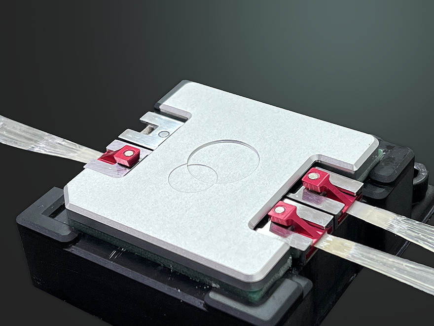
Photonic-Plug
Photonic-Bump
Wideband surface coupling
Detachable fiber connectivity
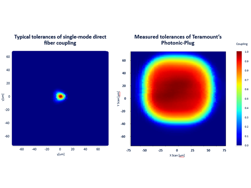
Self-aligning optics for large assembly tolerances
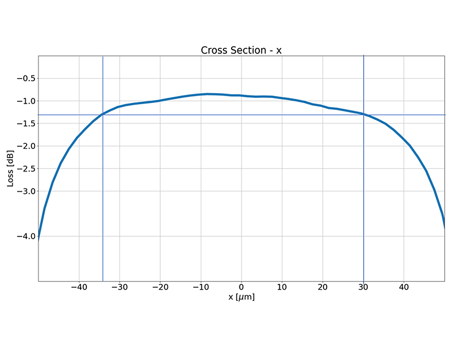
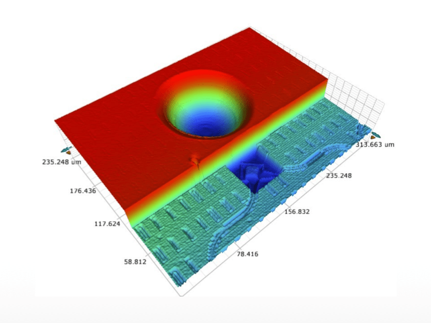
Teramount’s patented self-aligning optics technology, realized within the Photonic-Plug and Photonic-Bump components, offers better than ±30µm / 0.5dB of assembly tolerances when aligning single-mode (SM) or polarization-maintaining (PM) fibers to a silicon photonics chip.
Large assembly tolerances are a key issue for the enablement of large number of fibers passive assembly protocols. In addition, it is crucial for enhancing system thermal management.
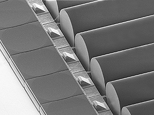
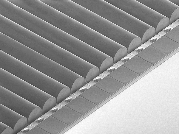
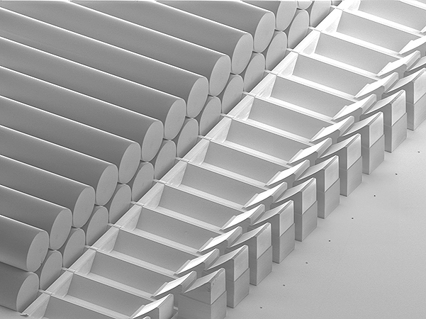
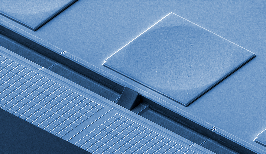
The Photonic-Plug
Incorporating wafer-level optical elements for enabling
Teramount’s patented “self-aligning optics” technology.
The Photonic-Plug makes use of wafer-level processes for
accurate placement of optical elements, thus shifting
accuracy requirements from assembly to wafer
manufacturing domain.
Unparalleled scalability with 127µm fiber pitch and 32+ SM/PM fibers
in a single-row configuration, or 64µm effective fiber pitch and 64+ SM/PM
fibers in a Double-decker configuration, thanks to the planar separation design,
which moves fibers from the PIC/Waveguide plane to the Photonic Plug.
Versatile design easily adapts to customer’s use-case and
PIC characteristics (Detachable vs. Bonded, Waveguide vs.
Grating Coupling, Fiber pitch & count, Expanded Beam, etc…).
with 32+ SM/PM fibers @ 127µm fiber pitch
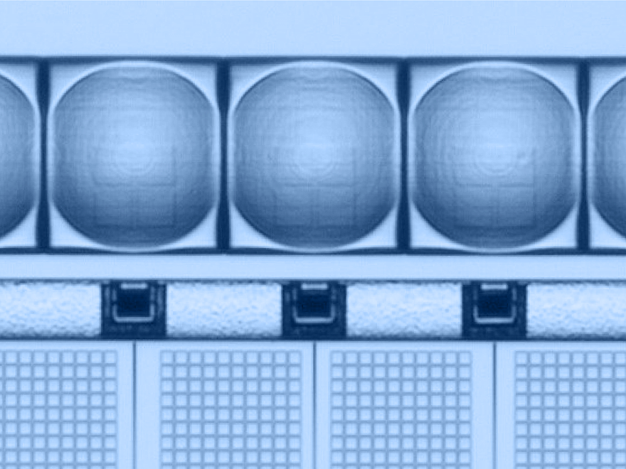
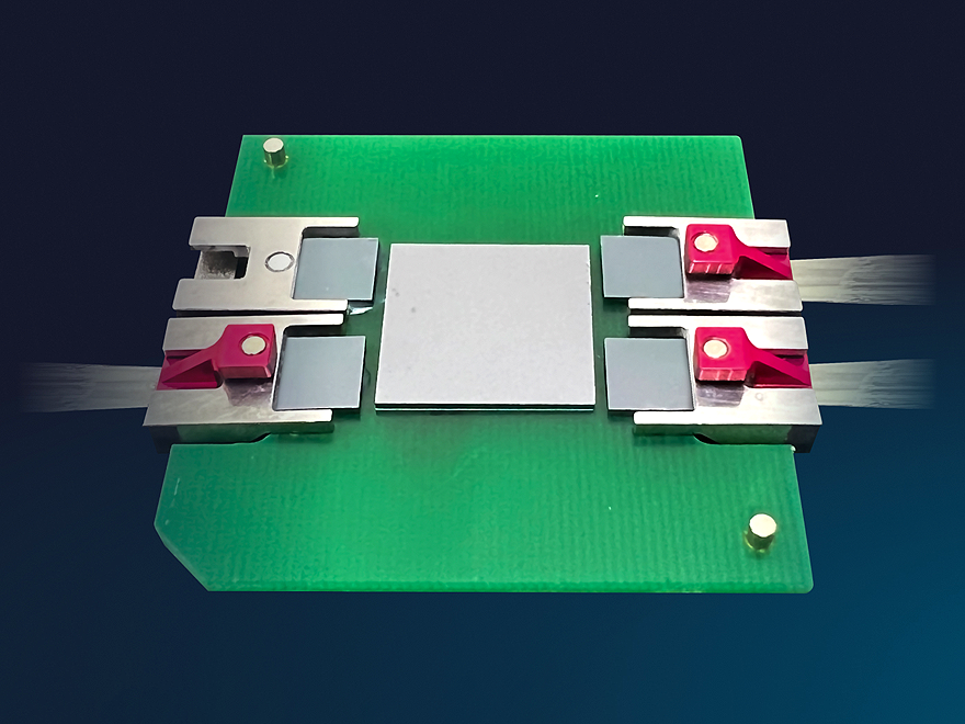
The Photonic-Bump
Teramount’s Photonic-Bump aligns photonics with standard semiconductor manufacturing, packaging, and testing flows. The Photonic-Bump is a wafer-level optical element attached on the customer’s silicon photonics PIC wafer and accurately placed relative to a tapered waveguide using wafer-level processes.
The Photonic-Bump enables the following key features:
- Beam deflection from a horizontal waveguide’s taper to a vertical axis for surface coupling. A deflector mirror is used to obtain wideband surface coupling and replace typical side-coupling.
- Mode-matching and spot-size conversion for matching waveguide and single-mode fiber spot sizes.
- Beam expansion for large assembly tolerances via “Self-aligning Optics” technology, when combined with Teramount’s Photonic-Plug.
- Wafer-level testing, allowing surface probing of silicon photonics wafers before dicing.
- Planar separation between fibers and silicon photonics chip for efficient optical and electrical packaging.
Teramount offers Photonic-Bump variants for both tapered waveguides and grating couplers, enabling unprecedented tolerances, passive assembly, and efficient wafer-level testing.
Wideband surface coupling
Teramount’s Universal Photonic Coupler incorporates beam-deflection optics optimized for WDM silicon photonics chips. It enables wideband surface-coupling, with the following key features:
- 32+ SM/PM fibers with 127µm pitch, connected to a customer’s PIC, for excellent scalability.
- Excellent Insertion Loss Performance per channel, under 1.5dB from facet to waveguide.
- Polarization Agnostic.
- Passive alignment, for a much higher assembly and testing throughput.
- Wafer-level Testing support, significantly increasing production yield
- 2.5/3D Packaging compliant, with full support for thinned PICs and Through-Silicon Vias
With Teramount’s wideband surface coupling, PIC designers finally have the ultimate fiber coupling solution suitable for high-volume manufacturing and can avoid the many limitations of legacy side coupling and narrowband surface coupling.
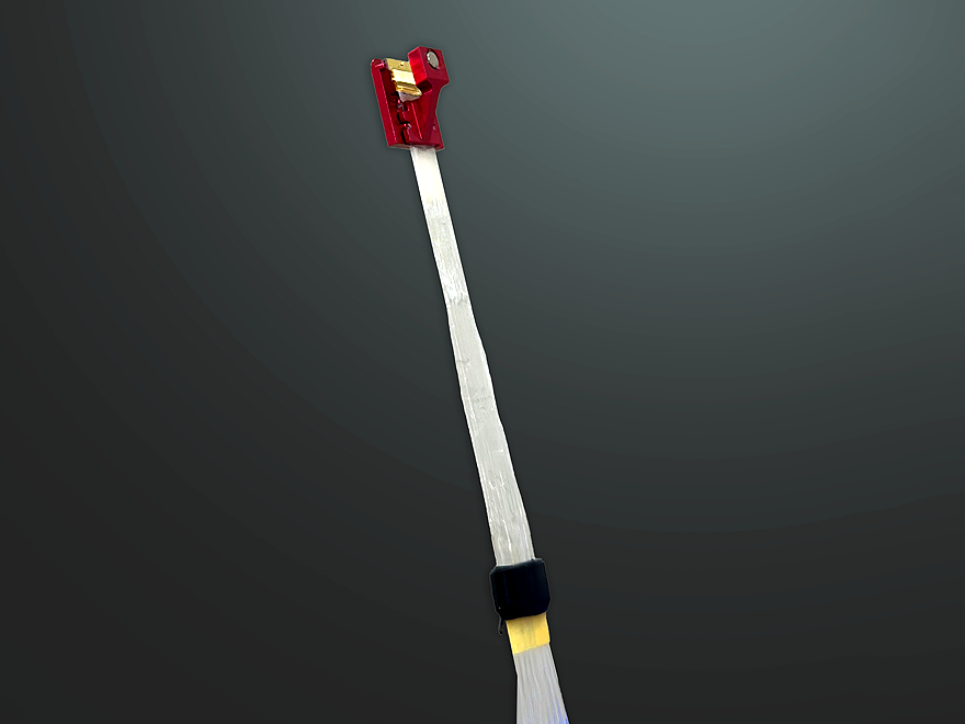
Detachable fiber connectivity:
Game changer for co-packaged optics
- Detachable Universal Photonic Coupler ushers in a new era of detachable and serviceable fiber connectivity for co-packaged optics.
- Post reflow assembly, improving packaging yield.
- Effective PIC testing pre- and post-fiber assembly through Teramount’s Photonic-Bump and planar coupling geometry.
- Large number of fibers for co-packaged optics and high bandwidth applications.
- No mid-board connector: One fiber ribbon from PIC to faceplate for higher optical throughput and improved insertion loss.
providing our customers with unparalleled high bandwidth and low power consumption”