TeraVERSE ®
A revolutionary detachable and serviceable fiber connectivity product for assembly of Single-mode (SM) and Polarization-maintaining (PM) optical fibers on a silicon photonics chip.
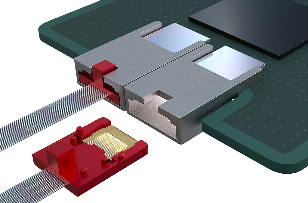
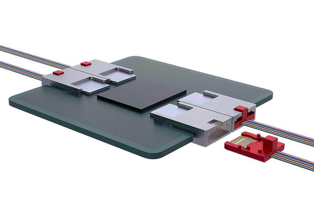
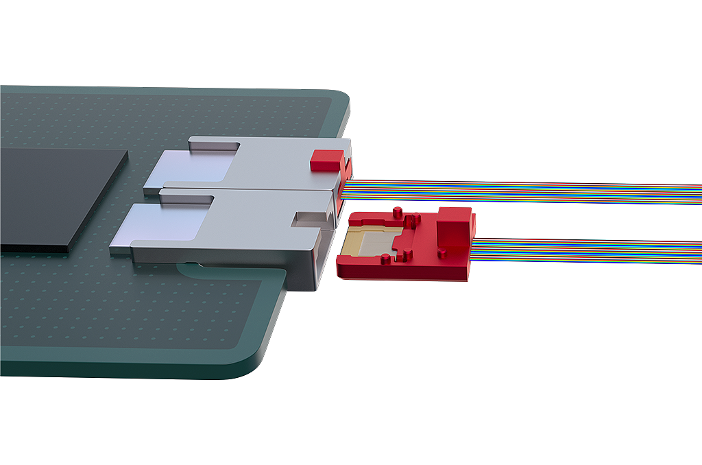
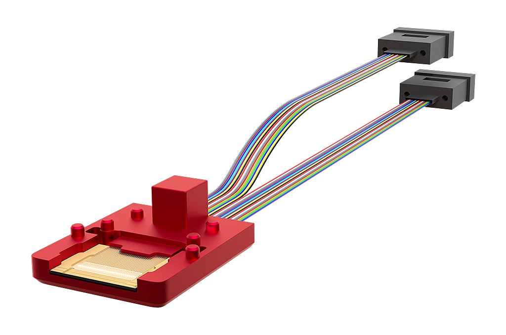
TeraVERSE provides a surface coupling solution comprised of Teramount’s detachable Photonic-Plug and a Photonic-Bump integrated into the customer’s silicon photonics chip using either Inverse Tapered Waveguides (wideband) or Grating Couplers (narrowband).
TeraVERSE is optimized for Co-Packaged Optics (CPO) use-case.
Key Features
Fully Integrated with standard semiconductor high-volume manufacturing and 2.5D/3D packaging flows, enabling vendors to finally manufacture silicon-integrated optics in high volume, with semiconductor-grade yield and reliability.
Surface Coupling for handoffs from both Inverse Tapered Waveguides (Wideband) and Grating Couplers (Narrowband). Enables Wafer-level and multi-stage testability.
Detachable solution perfect for CPO use-case. Post-reflow fiber connectivity and in-field serviceability significantly increase system yield and reliability.
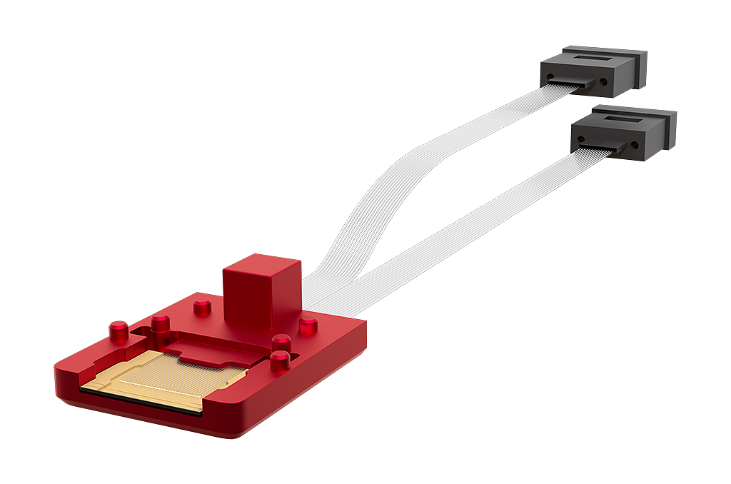
High Bandwidth Density with 127µm fiber pitch and 32+ fibers, or 64µm fiber pitch in a Double-Decker configuration and 64+ fibers per detachable Photonic-Plug.
Self-aligning Optics provide huge assembly tolerances of better than ±30µm / 0.5dB for assembling SM and PM fiber ribbon to a silicon photonics chip.
Modular Scalable Design allows 1:N connectivity between Socket & PIC and detachable Photonic-Plugs. Enables customers to scale up PIC density without impacting yield or solution simplicity.