How Silicon Photonics Is Tackling The AI Data Traffic Jam

Copper connections in large AI systems, where thousands of processors collaborate to train models or NurPhoto via Envato.
While hard questions about AI washing and hype are still being asked, AI continues to be in the spotlight in 2025, evidenced by its pervasiveness in many of the products and services displayed at the recently concluded CES. There’s also the jostling among companies like OpenAI, Anthropic, Google, new entrant DeepSeek and others in the AI arms race. Yet, with all its stride, AI’s unprecedented proliferation is also ushering in new challenges.
First, there are growing concerns on whether current processors can handle the massive data loads that AI applications generate. Behind the scenes of this data load problem is the over-reliance on traditional copper wires for transmitting data between processors. Although copper is remarkable, it struggles to meet the bandwidth and efficiency demands of modern AI workloads — slowing down data movement as a result.
Then there’s also the problem with the energy requirements of AI workloads, which further compounds global carbon emissions and pushes companies farther from the race to net zero by 2050. These problems create stiffer regulatory environments for AI to thrive and greatly hinder the value that businesses and individuals could get from the technology.
However, some experts say silicon photonics is a potential solution to some of these challenges. But what’s the big problem with copper — a great conductor that’s been very useful in chips for many decades — and why does this matter to the AI boom?
Out With The Copper
While processors have become exponentially more powerful, the copper cables linking them haven’t exactly kept up. In large AI systems, where thousands of processors collaborate to train models or analyze information, these copper connections are slowing things down. What’s more, they consume so much energy and introduce delays, limiting the system’s ability to grow.
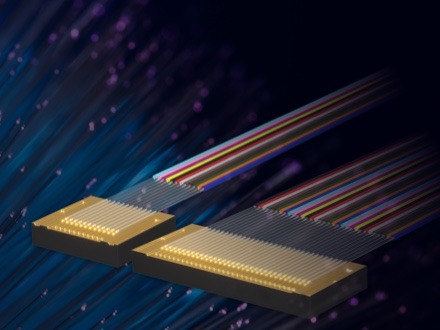
But that’s where silicon photonics — the technology that uses light, instead of electricity, to transmit data — comes in. With silicon photonics, replacing copper with optical fibers, data can travel faster, with less delay and using less power.
As Kazuhiro Gomi, CEO at NTT Research, noted in a previous article on Forbes, silicon photonics is good at linear, point-to-point data transport. “Getting optics to perform in a more nonlinear fashion, which is a requisite for computing, has been a focus of recent research and development,” he noted.
According to Dr. Hesham Taha, cofounder and CEO of Teramount — a company specializing in optical connectivity solutions — AI demands are growing faster than traditional connectivity can handle.
“Copper interconnects worked well for decades, but they are fundamentally limited by physics,” he said. “As AI systems become more complex, the limitations of copper are no longer sustainable for scaling. Silicon photonics isn’t just a nice-to-have but a necessity for the future of computing, particularly as the industry faces growing pressure to reduce power consumption and latency while supporting ever-larger data loads.”
Pros And Cons
Optical fiber, which is essentially a flexible glass that transmits light, carries much more data than copper cables and does so more efficiently — a feature that’s vital for data centers and AI clusters, which are the backbone of modern AI applications.
Reducing energy consumption and accelerating data transfer, silicon photonics allows data centers to process more complex tasks without overheating or latency. But this also comes with a problem: attaching optical fibers to silicon chips is a complex process that’s often time-consuming and requires costly alignment. And that’s because of something Atomica describes as “optical size mode mismatch.”
What does that mean? Imagine you’re trying to drink a milkshake with a straw, but the straw is either too big or too small for your mouth. If it’s too big, too much milkshake comes out and makes a mess. If it’s too small, it’s really hard to drink anything. This is kind of like optical fiber mode mismatch — when the light traveling through a fiber doesn’t match up properly with the tiny chip it’s supposed to go into.
Now, imagine you have a special adapter that automatically adjusts the straw size to perfectly fit your mouth every time. That’s what Teramount does with its Universal Photonic Coupler, which leverages self-aligning optics to simplify manufacturing. It automatically aligns the light coming from the fiber so it fits just right into the chip, making sure there’s no waste or loss. By aligning with standard semiconductor workflows, the company makes it easier for AI chipmakers to build optical connections into their products while reducing costs and improving scalability.
“The focus is on making optical connectivity practical for the semiconductor industry,” Taha told me. “By addressing the manufacturing challenges, we’re enabling the scalability that AI infrastructure demands.”
Future Outlook
Silicon photonics is already being used in high-performance computing and data centers, where fast, efficient data transfer is crucial. Its benefits extend to AI clusters, cloud computing, and telecommunications, with potential applications in other fields as the technology evolves.
The industry is also taking notice. For example, Lightmatter — a startup specializing in photonic data center networking chips — recently raised $400 million in a series D funding round, bringing its valuation to $4.4 billion. Other startups, as well as leading vendors and semiconductor giants like TSMC and Intel, are heavily invested in silicon photonics to meet the growing demand for advanced data transmission solutions in AI data centers.
“As AI continues to evolve, the need for faster, more efficient systems will only grow. Silicon photonics offers a transformative solution, addresses current challenges and paves the way for future innovations,” said Taha.