Optical Bump Nanoimprint Technology for Scalable Silicon Photonics Packaging
Check out our recent publication in Chip Scale Review where you can learn about Teramount’s groundbreaking Photonic Bump technology.
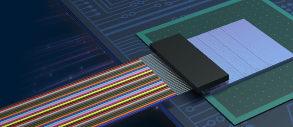
The Photonic Bump is a game-changing solution that creates a seamless integration between photonics and electronics.
Photonic Bump creates for the first time, an effective “through chip optical via” for seamless 2.5D and 3D photonics and electronics packaging. It holds the promise to align silicon photonics with the standard semiconductor manufacturing eco-system and to leverage silicon photonics to volume manufacturing for a variety of emerging applications.
Teramount and EV Group have collaborated to adopt wafer-level optics technologies in order to enhance silicon photonics packaging processes. Under this collaboration, nanoimprint lithography (NIL) has been used for wafer-level implementation of Photonic Bumps on silicon photonics wafers.
Read more about this exciting development on page 6 in Chip Scale Review here.