Silicon Photonics: Revolutionizing Data Centers at the Speed of Light
Data Centers, dedicated spaces used to house computer systems and related components, have become crucial for IT infrastructure and operations at scale. Businesses, computer networks, and individuals now use more data than ever. With demands soaring, Data Centers must revolutionize to keep up.
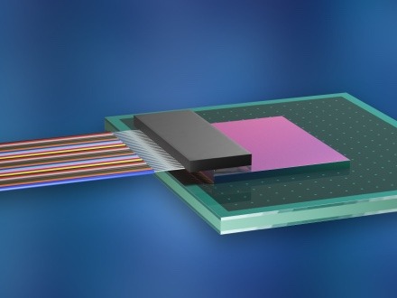
Grove Ventures’ latest investment, Teramount, develops a photonic plug for optics-silicon connectivity that may well be the game-changer that the data industry is looking for. In the Press Release announcing its funding round, the company stated that it “solves one of the most significant challenges of next-generation data center co-packaged switches…”. In simple words, there’s a revolution on its way to Data Centers. Switches, which route information in Data Centers involve an exciting technology called Silicon Photonics which will open the door to faster data transfers with lower power consumption.

Hesham Taha and Avi (Abraham) Israel, Founders of Teramount. Photo: Ilan Asaig
The Costs of Increased Data Usage: I/O Bottlenecks
The world’s appetite for data is growing exponentially. The explosion in AI, Machine Learning, and IoT is causing bandwidths and computing power resources in data centers to be used up. Mobile computing is especially demanding (fun fact: by 2013, the number of mobile phone subscriptions was just about the number of humans on Earth. In comparison, landline phones have never reached more than 25% of the global population). With the growing demand for data consumption, chips themselves have become faster (they still have Moore’s Law to abide by), allowing increased processing capabilities to ‘feed the beast’. Consequently, the use of fibers increased to transmit information faster.
Alas, the irony: We have reached a point where the chip can process information faster than the signal can be transmitted in and out. In other words, the chips became faster, but the optical signal (coming from the fiber) must still be converted to an electronic signal to communicate with the chip sitting on a board deep in the data center. And since the electrical signal still needs to travel some distance from the optical transceiver, where it was converter from light, to the processing and routing electronics — we’ve reached a point where the chip can process information faster than the electrical signal can get in and out of it. The I/O bottleneck in all its glory. No matter where one stands on the “Is More’s Law ending?” debate, it’s clear we are rapidly approaching the silicon chips’ limitations.
The Costs of Increased Data Usage:
Increased Power Consumption and Heat
We also know that the high toll all the data bandwidth is taking is on power consumption. And power consumption, our friends, unfortunately directly translates to heat (and cost). The industry has reached an inflection point where power is the ultimate limiting factor: Heating and power dissipation are enormous challenges for the microelectronics and computing industry. There is a reason some of the world’s largest Data Centers, including those of Amazon, Google, and Microsoft are located in Alaska and similar-climate countries: It’s cold there!
How desperate is the industry for a solution? In June 2018, Microsoft had encased a tiny data center with 12 racks of servers in a cylinder and threw it underwater — to sit on the ocean floor for up to five years. The idea was to use the sea as a natural coolant, helping to reduce the energy needed to run the center.
Just to put things in perspective, in 2009 Google argued that a search query consumes about 1 kJ of energy. Already, data centers use an estimated 200 Terawatt hours (TWh) each year — more than the national energy consumption of some countries. So, power consumption causes heat, and what’s causing power dissipation? Mainly, data transmissions. Transmitting data from a processor to a memory component or to another processor.
Optics-Based Computing: Less Energy Consumption, Faster Signals — But Until Recently, Immature
Optics-based computing uses less energy and can transmit data faster; instead of an electric bitstream, all you need to do is modulate the light to translate to 0 (no light) or 1 (light). It sounds so simple, doesn’t it? Let’s just get optics on a chip-scale, and let’s have it on silicon too. Oh, dear. Over multiple decades, the electronics industry has invested hundreds of billions of dollars on scaling manufacturing capabilities for silicon chips — equipment, processes, manufacturing flows and infrastructure. This has made silicon an inexpensive, robust platform for building Nano-sized structures. The costs of manufacturing silicon integrated circuits with embedded photonic elements, however, were what held back progress on this front. It was clear that optics had no justification unless it could be manufactured based on the existing infrastructure.
Welcome, Silicon Photonics
In the past decade, there has been a complete revolution in optics, a revolution very similar to the one microelectronics went through. The major breakthrough was the development of silicon photonics, a technology platform that relies on well-established semiconductors manufacturing techniques to make optical-integrated instead of electrical-integrated circuits. Today, one can define and print hundreds of thousands of optical elements using microelectronics lithography techniques. It may sound trivial, but 15 years ago, the idea that you could actually make optics using silicon was incomprehensible. When it finally manifested, it was widely and quickly embraced by the computing industry.
Traditional computing systems perform calculations with Integrated Circuits (ICs): transistor-based logic gates that use silicon’s semiconducting properties to control electrical current flow. Silicon Photonics, however, had to use a different approach. Silicon is transparent. In a silicon photonic system, light travels along waveguides: select channels etched into a pure Silicon dye using the same technology used to create electronic processors but in a much simpler design that is easier to manufacture. The light cannot escape these channels, so it follows the path etched into the silicon. Today, not only can we etch waveguides into silicon to transmit light, but we can also use the same approach to make components that allow us to adjust the properties of that light. Therefore, a silicon photonic system is also an integrated circuit, but one built to carry and manipulate light instead of electrical signals.
What’s Next?
All major microelectronics companies have started projects with Silicon Photonics. From fabs to the largest semiconductor companies through switch chipmakers, Silicon Photonics is the next big thing. Acquisitions and internal developments are also increasing: Cisco acquired Accacia for $2.6B and Luxtera for $660M, and Intel expanded its Silicon Photonics’ product offerings.
The Silicon Photonics market is projected to grow to $3 billion by 2025 (from $1 billion in 2020), growing at a CAGR of 23.4%, with Data Centers and High-Performance Computing applications expected to lead the market.
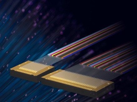
Some of the most exciting developments to look out for are focusing on transceivers (such as the ones developed by DustPhotonics), optical attenuators, switches, sensors, and integrated lasers. All of these developments will be re-designed to reduce cost, physical size, and operating power using Silicon Photonics elements.
Thanks to Silicon Photonics, optical input/output would be able to compete with, and ultimately outperform, electrical input/output.


