Teramount and Tower Collaborate on Photonic Elements Integration in High-Volume SiPh Wafer Manufacturing
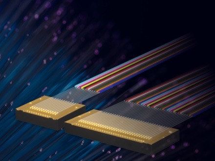
Teramount and Tower Semiconductor have recently announced their collaboration on integrating Teramount’s state-of-the-art self-aligning optics solution into Tower’s high-volume PH18 silicon photonic platform to produce silicon photonics “Bump-ready” wafers. This collaboration is an important step in realizing the vision of having photonics fully integrated into standard semiconductor manufacturing, by reorganizing SiPh manufacturing flow.
Teramount’s Photonic-Bump and Self-aligning optics technology provide huge benefits for silicon photonics Packaging and Design for Testability (DFT). For SiPh Packaging, Teramount brings significantly increased fiber assembly tolerances, passive alignment support and detachable fiber connectivity.
The Photonic-Bump’s unique feature of wideband surface-coupling supports critical testability capabilities, including wafer-level testing and multi-stage packaging testability – making sure DFT is no longer an afterthought in SiPh manufacturing – bringing yields up to par with standard semiconductor manufacturing.
Similarly to standard electrical bumps, customers will be able to select Teramount’s Photonic-Bump during the chip-design stage, and will be able to use Photonic-Bump process design kits (PDK) through Tower’s standard silicon photonics platform, benefitting them from scalable silicon photonics packaging, high-yield fiber assembly and fabrication at high-volume semiconductor manufacturing lines.
With this integration, Teramount and Tower will offer this capability to customers who need silicon photonics solutions for devices ranging from transceivers to high-bandwidth switches, as well as Co-Packaged Optics (CPO) for networking and advanced computing applications: GlobeNewswire


