Universal Photonic Coupling: A Deep Dive into the Next Generation of High Bandwidth Optical Connectivity
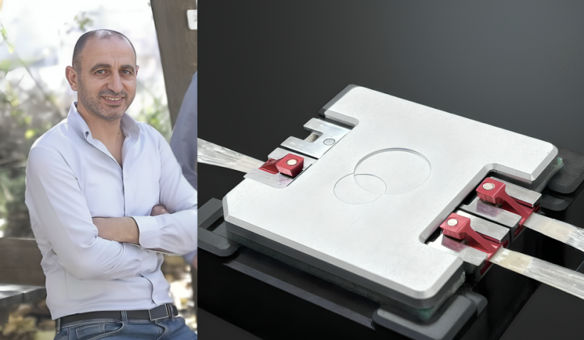
Dr. Hesham Taha, CEO of Teramount (Photo courtesy of Teramount)
The relentless pursuit of higher data throughput and efficiency in the digital age has brought the limitations of traditional data transmission technologies into sharp relief. As the world leans more heavily into high-performance computing (HPC), cloud computing, artificial intelligence (AI), and machine learning (ML), the need for a paradigm shift in high-speed data transfer solutions becomes undeniable. This shift is moving away from the copper-based interconnects of yesterday towards the optical chip connectivity of tomorrow. Teramount, a pioneering force in this transformation, is leading the charge with groundbreaking solutions that promise to redefine how optical fibers integrate with silicon photonics chips.
Against the backdrop of these industry-wide challenges, Teramount emerged with a clear mission: to facilitate the full realization of silicon photonics through innovative fiber-to-chip coupling solutions. “The transition to silicon photonics is a watershed moment for our industry, but its adoption has been held back by the technical complexities of fiber-to-chip packaging,” says Dr. Hesham Taha, CEO of Teramount. His vision was not just to navigate these complexities but to transform them into opportunities for innovation and advancement.
A Deeper Look at the Universal Photonic Coupler
Teramount’s overarching product is the Universal Photonic Coupler, which is designed to dramatically ease optical packaging, representing a radical departure from the status quo. “This coupler is the embodiment of our unique approach, combining simplicity with efficiency and precision in a way previously thought impossible,” Dr. Taha remarks, adding, “Its compatibility with wafer-level processes not only streamlines manufacturing but also ensures semiconductor-grade accuracy and yield for high-volume production.”
Building on the capabilities of the Universal Photonic Coupler, the company has unveiled TeraVERSE and TeraSPOT, each designed to meet the specific, evolving needs of the industry. TeraVERSE, aimed at Co-Packaged Optics (CPO), and TeraSPOT, for pluggable transceivers, tackle bandwidth and energy efficiency challenges in data transmission. Dr. Taha highlights the strategic vision behind these innovations, stating, “Our goal was to develop solutions that address current industry requirements while also laying the groundwork for future advancements.” These advancements include supporting applications such as chip-to-chip optical connectivity, underscoring Teramount’s commitment to versatility and forward-looking technology.
Redefining Fiber-to-Chip Assembly
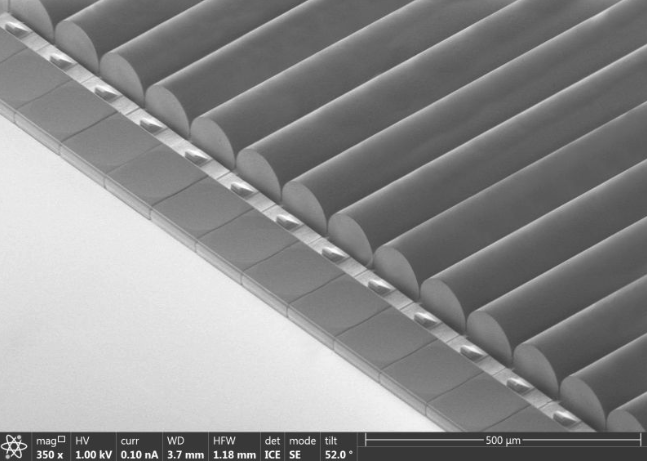
Teramount’s breakthroughs in fiber-to-chip integration incorporate the company’s unique Photonic-Plug and Photonic-Bump components, which have significantly advanced the company’s capabilities. This has allowed Teramoint to introduce a “self-aligning optics” technology that shifts precision requirements from assembly to wafer manufacturing, allowing for up to 100 times more relaxed fiber-to-chip assembly tolerances compared to other methods.
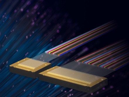
The Photonic-Plug is the fiber connector component of the Universal Photonics Coupler, currently supporting high bandwidth with a 127µm fiber pitch and 32+ SM/PM fibers, offering customizable solutions that cater to different customer needs and PIC characteristics through detachable or bonded designs. The Photonic-Bump component is a set of wafer-level optical elements on a glass carrier die attached to the customer’s silicon photonics wafer to enable efficient coupling through vertical beam deflection, beam expansion, and collimation for relaxed assembly tolerances. Additionally, it allows for unique wafer-level optical testing capabilities for high-yield manufacturing. The Photonic-Bump seamlessly integrates photonics with standard semiconductor fabrication, packaging, and testing processes and flows.
“These innovations mark a significant leap in optical connectivity. Our solutions surpass traditional methods by focusing on manufacturability, scalability and performance,” says Dr. Taha. The Photonic-Plug and Photonic-Bump are key to this strategy, offering versatile and reliable connections between optical fibers and silicon photonics chips, which facilitate high bandwidth, low-latency transmissions, and streamlined manufacturing processes.
Detachable Fiber Connectivity: A Leap in Optical Network Flexibility
Parallelly, detachable fiber connectivity represents a transformative step in the evolution of optical networks. This innovation, which includes the usage of a wafer-level self-aligning optics design with large fiber assembly tolerances, enables planar separation of the fiber connector for the silicon photonics chip, opening the door for mechanical detachability. Thus, it significantly bolsters maintenance and serviceability and dramatically streamlines manufacturability. By facilitating the post-reflow connection of thousands of fibers to the main processor, detachable connectivity offers a future-proof solution that keeps optical networks ahead of technological advancements. It ensures networks remain cutting-edge with minimal need for comprehensive system overhauls. This not only complements the wideband surface coupling’s advancements but also stands on its own as a critical enabler of adaptable, robust, and efficient optical communication infrastructures.
Embracing Wideband Surface Coupling for Advanced Computing
Integrating wideband surface coupling in high-performance computing and networking systems is pivotal, particularly for AI accelerators and advanced processors that demand high-speed optical links. Teramount’s Universal Photonic Coupler has revolutionized this domain by combining the broad bandwidth capabilities inherent in wideband coupling with the practicality of surface geometry. This not only overcomes the bandwidth limitations associated with traditional silicon photonics surface coupling but also avoids the complex packaging challenges posed by side-coupling methods. The result is a seamless blend of expansive bandwidth and simplified packaging, laying the foundation for the next generation of high-performance computing.
(Photo courtesy of Teramount)
Envisioning the Future of Optical Connectivity
Teramount has established meaningful collaborations with different ecosystem players, including foundries and OSAT’s. For example, In 2023, Teramount announced a significant collaboration with Tower Semiconductor. The collaboration with Tower is focused on leveraging Tower’s ‘Bump-ready’ wafers for scalable fiber-to-chip connections. According to the announcement from March, Tower successfully manufactured PH18 ‘Silicon Photonic Bump-ready’ wafers that demonstrated unparalleled performance in assembly tolerances when integrated with Teramount’sUniversal Photonic Coupler, solving a key bottleneck in the wider use of silicon photonics.
As Teramount continues to make headway in optical connectivity, Dr. Taha is confident its contributions are paving the path toward a future where data transmission is not constrained by the limitations of copper but propelled by the vast potential of light. “We are at the cusp of a new era in computing and data transmission, an era where our technologies will play a crucial role in unlocking the full potential of silicon photonics,” Dr. Taha envisions. This future, driven by Teramount’s innovations, promises to bring about significant advancements in AI, HPC, and beyond, transforming the landscape of the digital world.
————————————————————————————————————————————————————————————–
©2024 ScienceTimes.com All rights reserved. Do not reproduce without permission. The window to the world of science times.
* This is a contributed article and this content does not necessarily represent the views of sciencetimes.com