“We’ve Built the Missing Piece of the Puzzle”: Teramount’s Role in Solving AI’s Connectivity Challenges
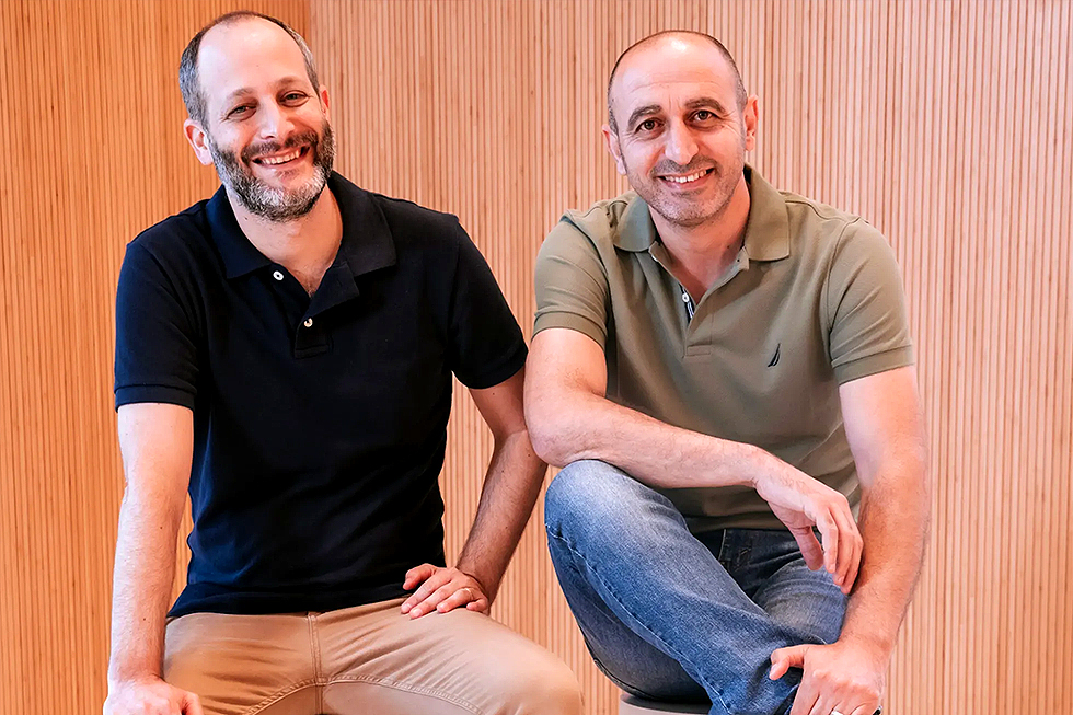
Teramount’s Co-Founders. Left: Avi Israel. Right: Hesham Taha. Courtesy of Teramount
As artificial intelligence (AI) and machine learning (ML) evolve at an unprecedented pace, the need for faster, more efficient data movement has become a critical challenge for the tech industry. Optical connectivity is emerging as a key enabler, and at the forefront of this transformation is Teramount: An Israeli startup co-founded by Dr. Hesham Taha and Dr. Avi Israel. Dr. Taha, CEO of Teramount, explains how the company is solving connectivity bottlenecks and how their journey has positioned Teramount as a key player in the future of AI infrastructure.
From Vision to Reality: Teramount’s Roots
“When Avi and I set up the company, we were focused on chip-to-chip optical connectivity,” recalls Dr. Taha. “At the time, people kept asking us, ‘Which customers would this product serve best?’ We knew exactly what we were building, but the challenge was identifying a suitable product segment. Back then, there were only a few niche use cases for silicon photonics. Now, with the AI revolution, there isn’t just a use case, but a crucial ecosystem need for our solution.”
The early days were challenging. The industry wasn’t ready for a platform approach to optical connectivity. But instead of following the traditional path of using legacy fiber assembly approaches with specialized equipment and processes, Teramount adopted a different philosophy: aligning photonics with the proven semiconductor manufacturing model. “Our mission was to make photonics work with standard semiconductor processes. That meant creating building blocks that could be integrated into existing semiconductor manufacturing and packaging workflows,” says Dr. Taha.
Hesham Taha
An innovative Approach to Connectivity
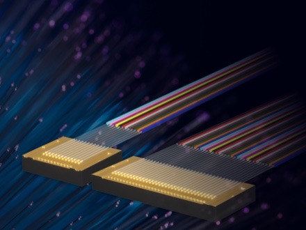
At the core of Teramount’s Universal Photonic Coupler platform is the “self-aligning optics” technology: a patented solution designed to integrate optical fibers seamlessly with silicon photonics chips. This innovation, along with the Photonic-Bump, enables unique passive alignment protocols, using standard semiconductor tools that reduce costs and increase scalability.
“Our Universal Photonic Coupler represents a paradigm shift,” Dr. Taha explains. “It isn’t just about performance; it is about creating a solution that aligns with semiconductor-grade processes that can be deployed in high volumes.”
This approach allowed Teramount to align photonics with the fabless semiconductor model, which separates design, manufacturing, and packaging. “The fabless model transformed the chip industry, and we realized we could extend that same model to silicon photonics,” says Dr. Taha.
Gaining Industry Momentum
Today, Teramount works with leading semiconductor foundries and OSATs (outsourced semiconductor assembly and test providers), including GlobalFoundries and Tower Semiconductor. These partnerships are crucial for ensuring that Teramount’s technology is available through standard supply chains.
“The traction we’ve gained from industry leaders is a testament to the scalability and reliability of our technology,” says Dr. Taha. “These partnerships are part of building a robust silicon photonics ecosystem, ensuring that our solutions meet the real-world demands of next-generation AI infrastructure.”
The market has taken notice. Companies like NVIDIA, Marvell, and Broadcom are investing heavily in optical connectivity. Recent funding rounds from companies such as Ayar Labs and Lightmatter highlight the urgency to address data movement bottlenecks.
The AI Boom: The Perfect Storm for Teramount
The surge in AI workloads has created a perfect use case for Teramount’s innovations. As models grow in complexity, the demand for high-speed, low-latency, and power-efficient data movement is skyrocketing.
“A high portion of the power in AI systems is consumed by connectivity rather than computation,” Dr. Taha explains. “Cooling these systems is a major cost in data centers. Our solutions seek to address this challenge by reducing power consumption and enhancing efficiency.”
The industry’s shift toward co-packaged optics (CPO) is well underway. But according to Dr. Taha, there are still significant hurdles. “CPO creates new constraints, and only the right building blocks can make it viable. That’s where Teramount comes in. Our technology makes it possible to scale optical connectivity in a way that fits seamlessly into existing manufacturing processes.”
Looking Ahead: Shaping the Future of AI Infrastructure
As the race for silicon photonics dominance intensifies, Teramount’s focus remains on scalability and reliability. “It is time to scale silicon photonics to meet the growing demand, particularly in AI and high-performance computing,” says Dr. Taha. “The challenge isn’t just about creating new technologies—it is about integrating them into existing manufacturing processes and ensuring they can be produced at scale to support next-generation infrastructure.”
Looking ahead, Teramount’s vision is clear. “We’ve built the missing piece in the puzzle,” Dr. Taha concludes. “Without scalable fiber connectivity, the silicon photonics revolution cannot realize its full potential. Our mission is to create reliable infrastructure solutions that will shape the next generation of AI and computing.”
With Teramount’s commitment to solving the critical connectivity needs of AI and HPC systems, the company is positioning itself to play a significant role in defining the future of optical connectivity—and by extension, the future of AI infrastructure.